Quickly Identify Parasitic Issues in Complex IC Designs Webinar 10am PST
Date March 24 2022
Time 10.00 am PDT - 11.00 am PDT
Location EDA Direct
Location Address Online Webinar
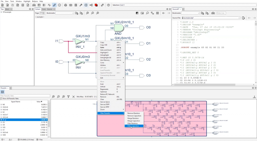
Parasitic-related design issues are becoming more prevalent as geometries get smaller. Identifying issues in parasitics through text files & layout or DRC/LVS tools is not intuitive, especially for the largest netlists.
Join this session to learn new methodologies & tools to assist in visualizing and debugging parasitic networks.
*Please Note: If you have registered for a past event, document or video, just Log in with your email. (Please do not try to re-register as you will see a registration error comment and will have to log in again).
What you will learn:
- Visualize and Analyze parasitic (RC) networks
- Quickly Remove/Merge & Filter R’s & C’s to perform what-if analysis
- Export reduced netlist for simulation
- See & cross-probe to largest to smallest capacitance
- Identify RC delays from from the extracted netlist
- Calculate pin to pin resistance
- Automatic Schematic generation from Spice, DSPF, SPEF, Spectre & more
- Full chip netlist tracing (top level integration and block level)
- Obtain detailed ‘insight’ to optimize for Speed and Power Consumption
- Very fast and can load extremely large netlists
Who should attend:
- Digital and Analog design and verification engineers
- Managers
- CAD Teams